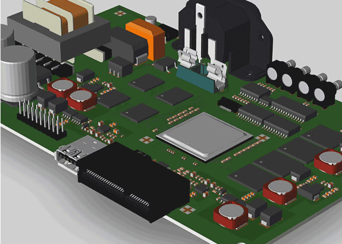
PCB (Printed Circuit Board) design and development is a pivotal aspect of electronics engineering, involving the creation of the physical circuit board that connects and supports electronic components. Designing a PCB requires a combination of electrical engineering knowledge and skill in using specialized software tools. Engineers meticulously plan the layout of components on the board, considering factors like signal integrity, power distribution, and thermal management. The goal is to create a compact, efficient, and reliable circuit layout. Once the design phase is complete, the development process involves manufacturing the actual PCB, which includes etching copper layers, drilling holes, and adding solder mask and silkscreen layers. PCB design and development are critical steps in the production of electronic devices, influencing their performance, size, and overall functionality. This field continues to evolve with advancements in technology, enabling the creation of increasingly complex and compact electronic systems.